
Lab Services > FIB Micromachining Laboratory
Sample Applications
FIB Milling Capability Sample Applications Imaging & Analysis
Fast focused ion beam (FIB) for cross-sectioning 3D-ICs
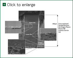
The plasma-FIB designed and built at Oregon Physics milled this 300x900µm cross-section structure in just under an hour. A 3µA beam of focused xenon ions has been used to polish this cross-sectioned face, removing >16 million µm3 of material at a rate of >5000µm3/s. The sample has then been tilted to 45° and imaged with a sub-100nm resolution, 100pA xenon beam. With the development of this new high throughput plasma-FIB, failure analysis of 3D-ICs is now possible with this FIB technique.
Milling this structure would take about 10 days with a conventional gallium FIB beam.
It would take 12 hours using a JEOL ‘Cross-section Polisher,’ with a mill rate of only 1.3µm/minute.
For additional information see:
Oregon Physics Application Note #2 3D-IC
Semiconductor device packaging
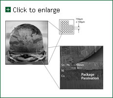
Here, ~250x106 µm3 of material has been precision milled from an in-situ I/O power delivery bump (VssIO). The cross-sectioned 750µm diameter solder ball and Under Bump Metallization (UBM) pad are imaged at a 45° incidence angle with a 100pA xenon beam.
For additional information see:
Oregon Physics Newsletter, December 2007
Oregon Physics, LLC
19075 NW Tanasbourne Dr., Suite 150
Hillsboro, OR 97124 USA
Phone: 503.601.0041 Fax: 503-992-6710 Email: info@oregon-physics.com
Web Design by Rareheron Web Design, Portland, OR